
Different from consumer electronic chips represented by mobile phones , automotive-grade chips have stricter requirements on service life, safety, reliability, and quality consistency.
From design to tape-out success, if everything goes well, pre-production can only be installed. The whole process takes about 3-5 years. The original Tesla took more than three years.
The ultimate goal of self-developed chips is to pursue scalability
Tesla is now looking to build the system from scratch, but it's not just developing its own AI chip, it's also developing a supercomputer.
At last year's AI Day, Tesla had released the Dojo supercomputer, but it was still fledgling, with only the first chip and training blocks, and the company was still pushing to build a complete Dojo Exapod.
Tesla also said that, in theory, the Dojo ExaPod will be the world's fastest AI training supercomputer.
From the presentation of Talpes in this seminar, each Dojo ExaPod integrates 120 training modules, built-in 3000 D1 chips, has more than 1 million training nodes, and has a computing power of 1.1EFLOP* (petaflops per second). point operation).
The custom-built supercomputer is expected to improve Tesla's ability to train neural networks using video data and is critical to Tesla's Autopilot capabilities.
If you want to complete a series of constructions, you need self-developed chips
It is Tesla's self-developed neural network training chip D1 chip that enables Dojo to complete the task of training AI algorithms.
But the Dojo supercomputer launched at Tesla AIDay last year is based on Tesla's self-developed D1 chip.
The Tesla D1 chip has the following features:
①2D Mesh architecture;
②Many-core architecture with vector and matrix computing acceleration units;
③ Integrated storage and computing architecture (near storage computing).
Compared with other chips in the industry, the performance is improved by 4 times at the same cost, the performance is improved by 1.3 times at the same energy consumption, and the space occupation is reduced by 5 times.
Each DojoExaPod integrates 120 training modules, built-in 3000 D1 chips, has more than 1 million training nodes, and has a computing power of 1.1EFLOP* (petaflops per second).
.jpg)
The Dojo AI system is fully self-developed and self-developed dedicated instruction set
The so-called Dojo is a supercomputer developed by Tesla, which can use massive video data to complete [unsupervised] annotation and training.
Essentially, Dojo is built from a completely custom architecture covering compute, networking, input/output (I/O) chip-to-instruction set architecture (ISA), power delivery, packaging, and cooling.
Often, startups want to build AI chips of one or a few chips per system.
Clearly, Tesla is focused on bigger scale.
What's even more exciting is that it's not only using commercially available systems, but is building its own chips and systems.
The development process of Tesla’s Dojo AI system is similar to that of in-vehicle systems. Tesla itself employs researchers to develop related chips and systems for it.

The Dojo AI system adopts a distributed architecture
The Tesla Dojo AI system adopts a distributed architecture, and each Dojo node has its own CPU, memory and communication interface .
While each node has 1.25MB of SRAM, each node is then connected to a 2D grid.
The Dojo interface processor sits at the edge of the 2D grid and has 11GB of SRAM and 160GB of shared DRAM per training block.
The Dojo core has an integer unit that borrows some instructions from the RISC-V architecture, and has a whole bunch of additional instructions that Tesla created itself.
The Dojo instruction set supports 64-bit scalar instructions and 64 BSIMD instructions, it includes primitives for handling data transfer from local memory to remote memory, and supports semaphore and barrier constraints.
This is to make memory operations conform to instructions to run not only in D1 cores, but also in a collection of D1 cores.
Each Dojo node has a core and is a full-fledged computer with CPU-specific memory and I/O interfaces.
D1 means it supports instruction-level parallelism in its core, and like most chips today, it even has a multi-threaded design to drive more instructions through that core.
D1 processor architecture: Each D1 processor consists of 18x20 D1 cores. There are 354 D1 cores available in each D1 processor.
For the sake of yield and processor core stability, the D1 processor is manufactured by TSMC , using a 7nm manufacturing process, with 50 billion transistors and a chip area of 645mm².
This size is smaller than Nvidia's A100 (826mm²) and AMD Arcturus (750mm²).
However, each core is a complete CPU with matrix computing capabilities, and its computing flexibility is far beyond that of GPUs with many-core architectures, which also brings extremely high costs.
·D1 core structure: From the structure of each D1 core in the 18x20 array, each D1 core is processing with vector computing/matrix computing capabilities.
It has complete instruction fetching, decoding and execution components. The processor runs at 2GHz and has four 8x8x4 matrix multiply calculation units.
D1 processor instruction set: based on the RISC-V architecture ISA to expand.
The D1 core has two standard computing formats, FP32 and FP16, as well as the BFP16 format that is more suitable for Inference.
To achieve improved performance in mixed-precision computing, the D1 also uses the 8-bit CFP8 format for lower precision and higher throughput.
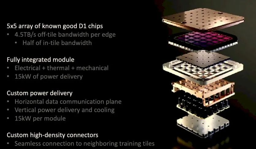
·D1 training block architecture: Each D1 training block is arranged by a 5x5 D1 chip array, interconnected in a two-dimensional Mesh structure.
The on-chip cross-core SRAM reaches an astonishing 11GB, which is a very typical near-memory computing architecture. Of course, the power consumption has also reached an astonishing target of 15kW.
The 40 I/O chips on the outer edge of each training module achieve an aggregate bandwidth of 36TB/s, or a spanned bandwidth of 10TB/s.
Car companies have never been so high on chips as they are today
Manufacturers of self-driving cars are starting to realize that teaching cars to drive themselves in a complex world is always changing and will require more supercomputing.
First, because of the two-year "chip shortage" in the world, the OEM's emphasis on supply chain security has reached an unprecedented height;
Second, because intelligence is a necessary condition for new energy competition, the era of software-defined vehicles has arrived.
As the first car company to jump out of Mobileye's closed business model, Tesla started the self-driving chip research and development project as early as early 2016, and officially launched it in mass production vehicles in 2019.
Driven by Tesla, leading new forces such as Weilai, Xiaopeng and Ideal have followed suit.
In 2021, they announced their own self-research plans for autonomous driving chips. Ideal even set up [Ideal Intelligence] in Mianyang three months ago.
Entering this year, the autonomous driving chip [Lingxin 01] has also entered the integration verification stage, and will be tested in real vehicles in the second quarter of next year.
end:
After Tesla's achievements in chip and supercomputing development, it may encourage more car companies to join in chip and supercomputing research and development, vigorously develop independent innovation capabilities, and enhance corporate competitiveness.